

Summary of the final report of the research project: Alternative densification processes for nanoparticle inks printed with digital printing processes for planar MID (AVerdi)
In the research project “Alternative densification processes for nanoparticle inks printed with digital printing processes for planar MID – (AVerdi)” silver nanoparticle inks were printed with the digital printing processes inkjet and aerosoljet on thin polymer films as well as on injection-moulded polymers and the influence of photonic sintering processes in the form of near infrared (NIR) or ultraviolet (UV) radiation on the electrical conductivity and adhesive strength of the printed structures compared to convective sintering was investigated.
NIR lamps from adphos Digital Printing GmbH and UV lamps from Dr. Hönle AG UV technology were used for this purpose. The aim was to achieve with the photonic sintering process an electrical conductivity comparable to or better than that of the furnace process, with good adhesive strength and a significantly reduced sintering time for all substrate types. Sintering on thermally sensitive substrates such as polyethylene terephthalate (PET) was of particular interest.
The results obtained in the research project have shown that photonic sintering processes are significantly better suited for sintering digitally printed structures on thermally stable substrates than the established convection processes, since in most cases higher electrical conductivity could be achieved with a significantly reduced sintering time. Different inks and a variety of substrate materials were used. The material portfolio was reduced in the course of the project.
In final studies, Clariant TPS 50 and PARU PG-007 inks and injection-molded substrates of liquid crystal polymer (LCP) and polyamide 6 (PA 6) were used for aerosol jet printing. The inks ANP DGP 40TE-20C, Clariant TPS 35 and GSB choice LAB 2423 and substrate films made of PET and polyimide (PI) were used for the inkjet process.
In investigations on the properties of the ink Clariant TPS 35, which can be processed in the inkjet process, photonic sintering was able to achieve an electrical conductivity relative to bulk silver in the range of approx. 17 % to approx. 24 % on PI at a sintering time of 2 s to 5 s, whereby in the furnace process a conductivity of approx. 12 % to approx. 14 % was achieved after one hour at 200 °C. Scanning electron microscope images of photonically sintered samples showed a significantly better sintering degree compared to the furnace process. The adhesive strength after photonic sintering is comparable to oven-sintered samples. On PET with the ink ANP DGP 40TE-20C a conductivity of approx. 6 % to approx. 7 % could be achieved by NIR radiation after one second. In the furnace process a conductivity of approx. 3 % to approx. 4 % relative to bulk silver was achieved after 5 min at 150 °C. SEM images showed that no sinter neck formation had yet taken place here, so that the conductivity was most likely achieved via initial contacts between the silver nanoparticles. Very good adhesion values were achieved with both sintering processes.
In tests on the properties of the ink PARU PG-007, which can be processed in the aerosol jet process, photonic sintering was able to achieve a conductivity relative to bulk silver in the range of approx. 13 % to approx. 35 % on LCP at a sintering time of 2 s to 60 s, whereby in the furnace process a conductivity of approx. 25 % was achieved after one hour at 150 °C. For this material combination, the adhesive strength was classified as poor after all sintering processes. On PA 6, a conductivity of approx. 17 % to approx. 19 % relative to bulk silver with good adhesive strength could be achieved with the same ink by photonic sintering, whereby in the furnace process after one hour at 150 °C approx. 16 % conductivity was achieved with poor adhesive strength.
Overall it was found for both printing processes that the sintering time could be significantly reduced by photonic sintering. In most cases better electrical conductivity values could be achieved than in the furnace process. Thus, the sintering processes investigated in the research project are well suited to achieve high conductivities with good adhesive strength on thermally resistant substrates. On thermally sensitive substrates, on the other hand, it was possible to achieve low conductivities with very good adhesive strength, which could be interesting for sensor applications, for example.
The IGF Project 19605 N of the Research Association 3-D MID is funded via the AiF within the framework of the program to promote joint industrial research (IGF) by the Federal Ministry of Economics and Energy on the basis of a resolution of the German Bundestag.
Contact
For further information on this completed research project, please contact the office by phone or e-mail. E-Mail to the office
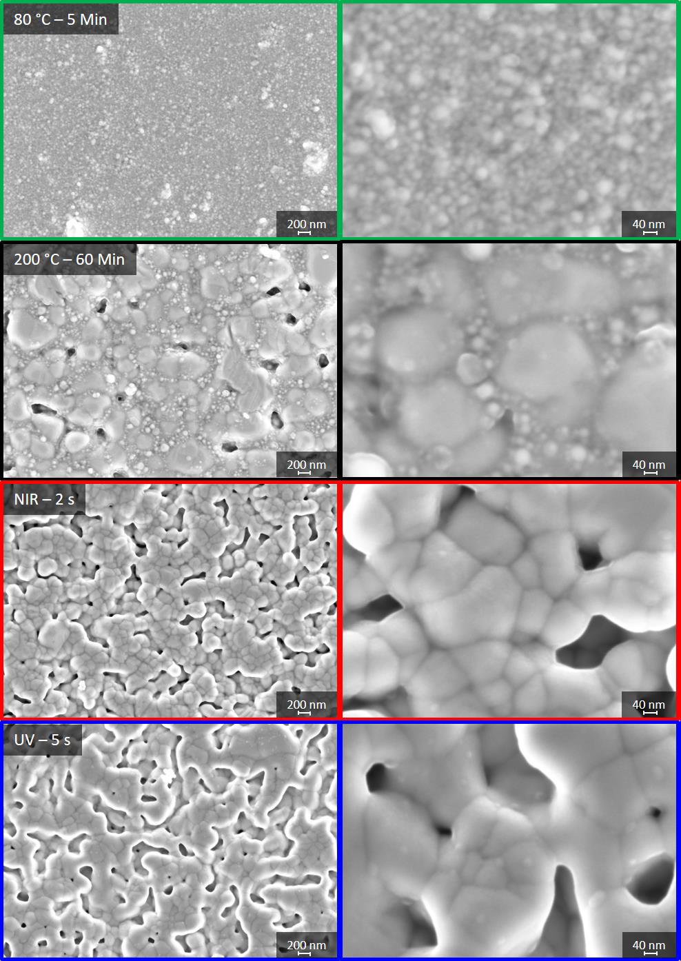
Figure 1: Clariant TPS 35 on PI: Scanning electron microscope images: after pre-drying at 80 °C – 5 min, after oven sintering 200 °C – 60 min, after NIR sintering – 2 s and after UV sintering – 5 s.

