Description
Optical data transmission in electro-optical printed circuit boards makes it possible to achieve high data rates over short distances. In addition to fiber-based and lithographic manufacturing processes, it has recently also become possible to optically functionalize printed circuit boards using printing technology in a cost-effective and productive manner. However, a major challenge remains the implementation of the assembly and interconnection technology for optical coupling and decoupling in optical waveguides, which is subject to higher requirements than conventional electronic assembly technology. The qualified optical emitters (laser diodes) and receivers (photodiodes) are surface active and therefore require a deflection of the light beam or a vertically rotated mounting position for face-to-face coupling. Common packages that implement a rotation of the device do not have the necessary shape functionalizations that would be required for a passive optical assembly. 3D-Mechatronic Integrated Devices (MID) offer versatile shape and trace structures with high geometry quality and are therefore particularly well suited as optical coupling submounts for printed optical fibers. The main challenge for research is to verify whether a passive assembly process can be used for alignment by synchronizing and designing the form and function of the MID and the electro-optical printed circuit board. Furthermore, it has to be investigated to what extent an MID can guarantee electrical shielding, the use of integrated driver electronics, thermal management and packaging for the optical components in view of the geometrically predefined shape and the limited installation space.

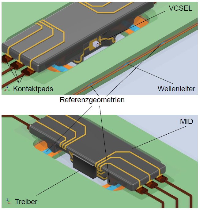
Figure: Concept for passively contacted waveguides; Source: Leibniz Universität Hannover (ITA)
In this project, the coupling point and the MID itself are to be adapted and investigated on the basis of printed optical circuit boards so that a passive assembly process can then be used to implement electro-optical coupling. For this purpose, different contacting and placement concepts are developed within a tolerance chain analysis and evaluated by means of optical coupling simulations. Based on this, a layout for the printed circuit board and the EMF including conductor tracks can be designed, which is then implemented as a prototype. The MID is adapted using prototyping and/or post-processing processes so that it corresponds to the planned concept. Subsequently, the optical components on the MID as well as the submount on the PCB will be assembled and the coupling quality will be characterized by means of active alignment investigations. Submount development will continue iteratively until sufficient optical coupling into an integrated optical waveguide is achieved. Building on these results, a standardized MID submount is constructed based on the laser direct structuring (LDS) method and the optical coupling efficiency is validated.
Research Objective
The research objective of this project is the implementation of a passively mountable optical interface for data communication in printed circuit boards. The main innovation here is the application and functionalization of an MID to the novel requirements of the optical coupling scenario using surface active diodes (transmitter/receiver). The research project combines the electrical design of the conductor paths on the submount for gigabit/s transmission rates, the assembly of diodes on the MID submount referenced to alignment structures and the precise assembly of the MID submount on the end faces of printed optical fibers. Position tolerances of less than 20 μm are to be achieved and, in addition, coupling to single mode waveguides is to be experimentally verified. The optical coupler MID submounts are to achieve optical data transmission rates of up to 2 Gbit/s with coupling losses of less than 3 dB and be adaptable. The intended standardization for a mass production of LDS MID enables different coupling scenarios.
Benefits and economic significance for SMEs
The industrial application potentials are in the field of short distance communication systems as well as galvanic isolation in EMC sensitive areas. In this respect, new mass markets can be opened up in the optronic sector and in data communication, which rely on integrated optical data transmission. The industrial implementation possibilities after the end of the project lie in the implementation of a novel process chain in which SMEs can map various sub-processes (design, injection molding, laser sintering, metallization, opto-packaging, assembly, …) within the value chain. A standardized coupling system offers a significant competitive advantage due to its unique position on the market.
Research Institutes
For further contact details, please contact the office. See contact details
Leibniz Universität Hannover
Institut für Transport- und Automatisierungstechnik (ITA)
Project Accompanying Companies
The Research Association 3-D MID is still looking for companies to accompany the project. If you are interested, please contact the office. See contact details