

Two exciting presentations from industry and research await you at the 9th MID Day on February 8, 2023. The online event begins at 4 PM (CET) and is open to all free of charge. First, Dr.-Ing. Timo Kordass will give the presentation “Laser-assisted process for selective metallization of epoxy resin-based duromers to increase integration density for three-dimensional mechatronic package assemblies”.

Figure 1: MIDster; Source: FAPS
The miniaturization of the circuit geometries on three-dimensional mechatronic integrated components (3D-MID) show challenges due to thermomechanical stresses between polymer substrates and the chemical deposited metal layers.
The presentation describes research results on the use of alternative epoxy resin-based thermosets that can be processed in transfer and injection molding process. Compared to the thermoplastic materials such as polycarbonates, polyamides and liquid-crystalline polymers, thermosets offer a significantly lower coefficient of thermal expansion (CTE). The focus is on the development of an activation process for laser-assisted, selective-additive metallization of fine-pitch circuit layout on non-conductive substrates. With expanded range of available substrate materials, MID applications can be applied in the area of packaging assemblies with high degree of miniaturization.
Michael Hümmer from the TH Nuremberg will then present the “PrInterfaces” research project – technologies for high-quality contacting of printed structures for the establishment of Level 3 connections between electronic assemblies.
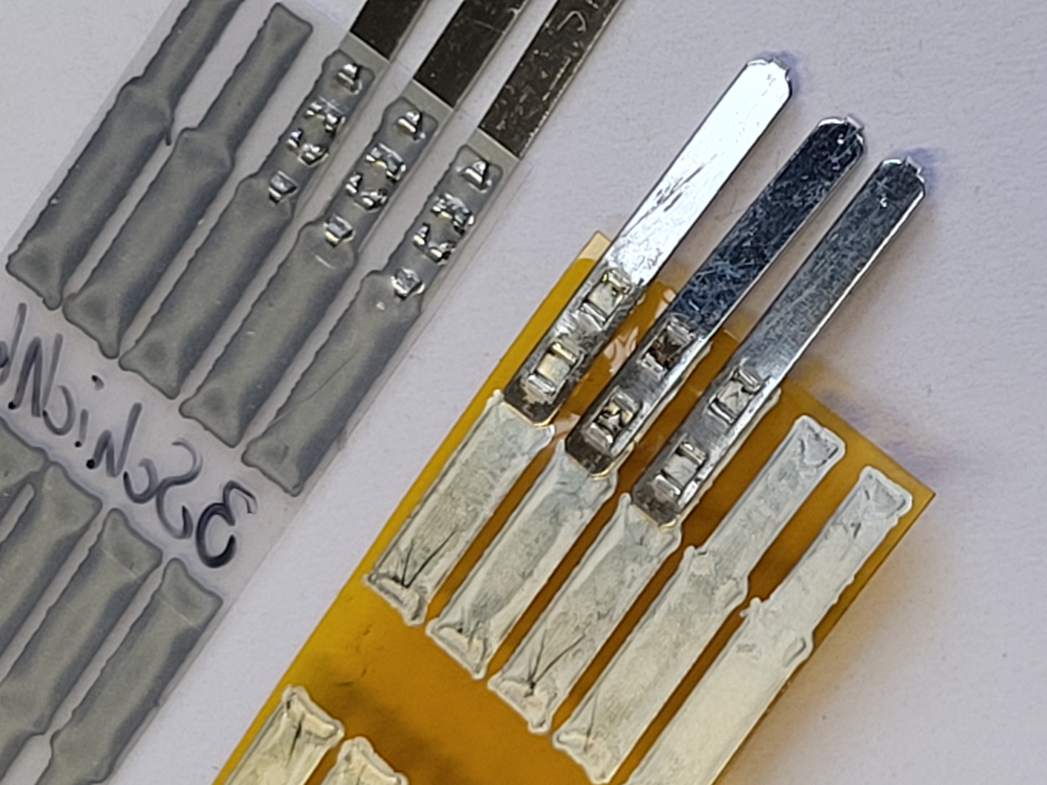
Figure 2: Conductor structures produced by inkjet printing and contacted via penetration crimp on PI and PET substrates; Source: TH Nuremberg
The technical and economic performance of printed electronics technology is superior to that of established production techniques for some aspects of electronic system design under certain conditions. One example of this is the production of the conductor pattern. However, the complete, print-based realization of an electronic system is either not yet technically feasible or not economically viable. In this respect, it may be necessary to connect a printed circuit diagram with other components, such as those produced using established production techniques, in order to ensure the overall functionality of the electronic system. This may also require connection at board level, i.e. from board to board (level 3). Known joining technologies of established electronics production are available for joining. However, their suitability for high-quality contacting of printed conductor structures is unknown. This is because such structures have different components and properties compared with conventional copper layers on printed circuit boards. Consequently, this changes the contacting / joining system. The effect of the changes on the interconnection technology and its production parameters must be investigated in the context of reliable interconnections. For this purpose, the suitability of stirrup brazing, ACF heat sealing, crimping and press-fit in combination with aerosol jet, piezo jet, inkjet as well as screen printed structures will be verified. The effects of the material combination (substrate, track, interconnection), process parameters (sintering/hardening, contacting) as well as the track properties on the interconnections are comprehensively characterized. The long-term behavior of the interconnections is also determined.
More information about the MID Days can be found here.
